We can see a row of golden conductive contacts on the computer memory module and graphics card, and each part is a golden finger.
We generally electroplate nickel and gold, the thickness can reach 3-50u". Features, superior conductivity, oxidation resistance and wear resistance, is widely used in gold finger PCBs that require frequent insertion and removal or PCBs that require frequent mechanical friction On the board. Another way is to deposit gold, the thickness is conventional 1u", up to 3u". Features, superior conductivity, flatness and solderability, is widely used in the design of buttons, bonded IC, BGA, etc. For high-precision PCB boards, for gold finger PCBs that do not require high wear resistance, you can also choose the whole board immersion gold process. The cost of the immersion gold process is much lower than that of the electro-gold process. The color of the immersion gold process is golden yellow.
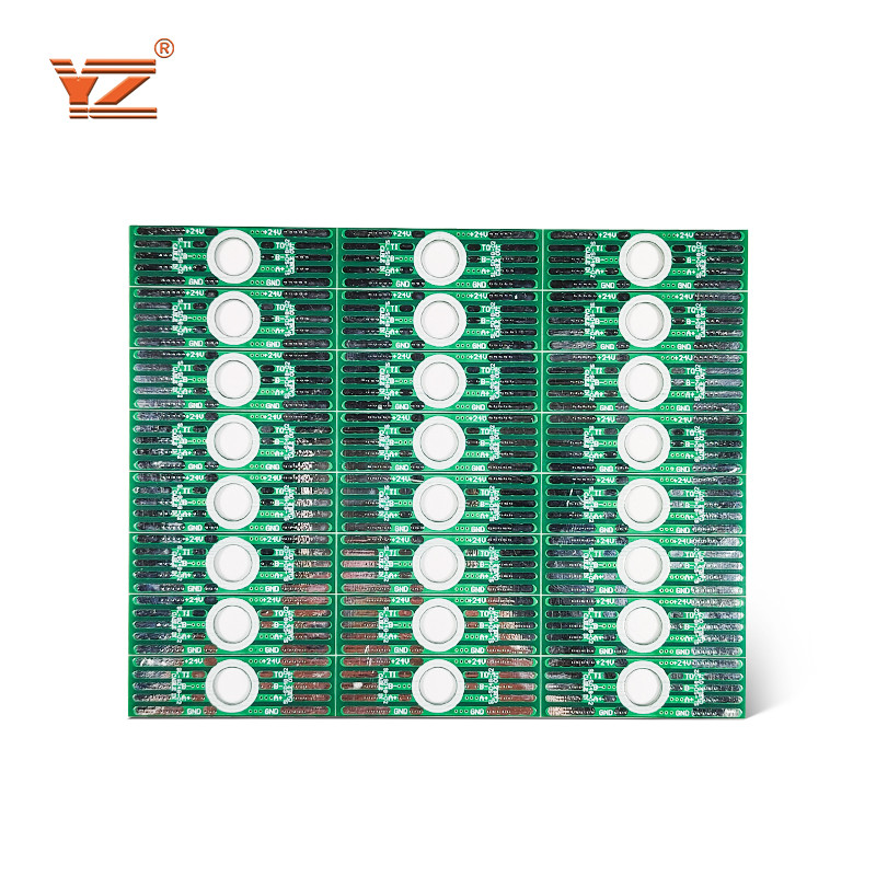
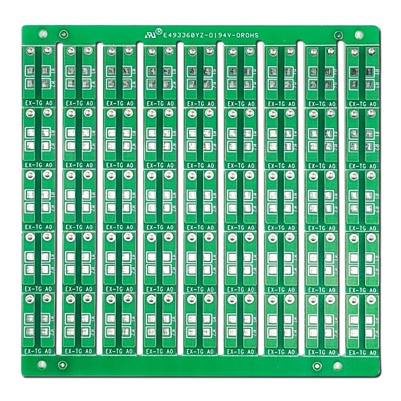
FR4 PCB can be any layer count but rely on conventional drilling and plating technology.
-
FR4 PCB up to 40+ layers
-
Wide range of laminate options including high temperature, low loss, and lead-free laminates
-
Mixed dielectric (hybrid) constructions
-
Panel size up to 30″x 55″
-
Embedded coin or metal core and metal-backed MLB
-
Panel thickness up to.450″
-
RF and microwave circuits
-
Heavy copper (10 oz. outer layer / 5 oz.
inner layer)
-
Embedded, distributed and discrete passive components