Specifications
Brand Name :
ZMSH
Model Number :
Silicon carbide wafer
Place of Origin :
China
Delivery Time :
2 weeks
Payment Terms :
100%T/T
EPD :
≤1E10/cm2
Thickness :
600±50μm
Particle :
Free/Low Particle
Edge Exclusion :
≤50um
Surface Finish :
Single/Double Side Polished
Type :
3C-N
Resistivity :
High/Low Resistivity
Diameter :
2inch 4inch 6inch 8inch
Description

2inch 4inch 6inch 8inch 3C-N SiC Wafer Silicon Carbide Optoelectronic High-Power RF LEDS

Description of 3C-N SiC Wafer:

Compared to 4H-Sic, although the bandgap of 3C silicon carbide

(3C SiC) 2inch 4inch 6inch 8inch 3C-N SiC Wafer Silicon Carbide Optoelectronic High-Power RF LEDS
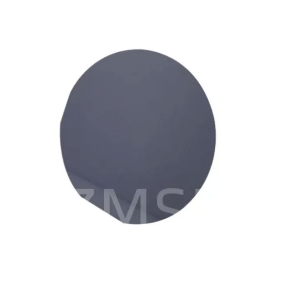
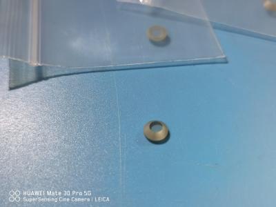
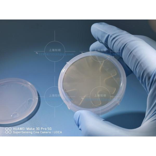
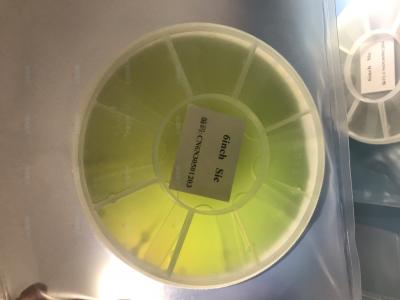
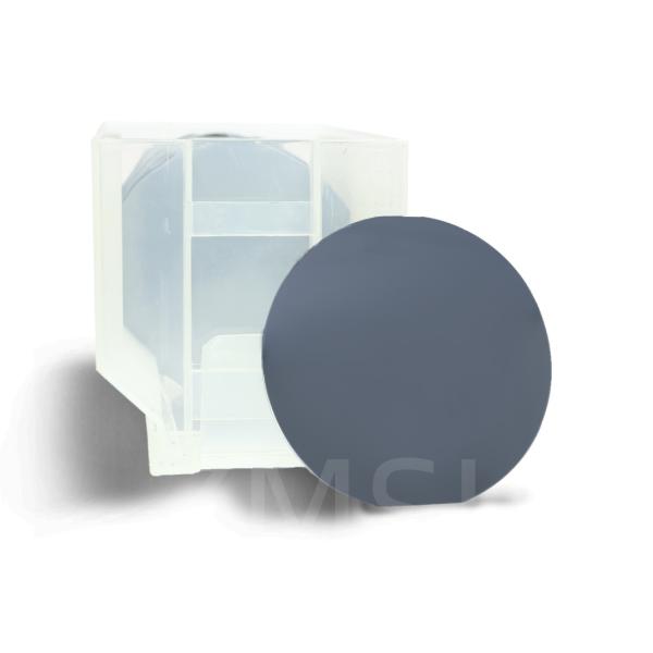
is lower, its carrier mobility, and thermal conductivity. and mechanical properties are better than those of 4H-SiC. Moreover, the defect density at the interface between the insulating oxide qate and 3C-sic is lower. which is more conducive to manufacturing high-voltage, highly reliable, and long-life devices. At present, 3C-SiC-based devices are mainly prepared on si substrates with large lattice mismatch and thermal expansion coefficient mismatch between Si and 3C SiC resulting in a high defect density, which affects the performance of devices. Moreover, low-cost 3C-SiC wafers will have a significant substitution impact on the power device market in the 600v-1200vvoltage range, accelerating the entire industry's progress. Therefore, developing bulk 3C-SiC wafers is inevitable.

The character of 3C-N SiC Wafer:

1. Crystal Structure: 3C-SiC has a cubic crystal structure, unlike the more common hexagonal 4H-SiC and 6H-SiC polytypes. This cubic structure offers some advantages in certain applications.
2. Bandgap: The bandgap of 3C-SiC is around 2.2 eV, making it suitable for applications in optoelectronics and high-temperature electronics.
3. Thermal Conductivity: 3C-SiC has high thermal conductivity, which is important for applications requiring efficient heat dissipation.
4. Compatibility: It is compatible with the standard silicon processing technologies, enabling its integration with existing silicon-based devices.

Form of 3C-N SiC Wafer:

Propery N-type 3C-SiC, Single Crystal
Lattice Parameters a=4.349 Å
Stacking Sequence ABC
Mohs Hardness ≈9.2
Therm. Expansion Coefficient 3.8×10⁻⁶/K
Dielectrc Constant c~9.66
Band-Gap 2.36 eV
Break-Down Electrical Field 2-5×10⁶V/cm
Saturation Drift Velocity 2.7×10⁷m/s

Grade Zero MPD Production Grade (Z Grade) Standard Production Grade (P Grade) Dummy Grade (D Grade)
Diameter 145.5 mm~150.0 mm
Thickness 350 μm ± 25 μm
Wafer Orientation Off axis: 2.0°-4.0°toward [1120] ± 0.5° for 4H/6H-P, On axis:〈111〉± 0.5° for 3C-N
Micropipe Density 0 cm-2
Resistivity ≤0.8 mΩꞏcm ≤1 m Ωꞏcm
Primary Flat Orientation {110} ± 5.0°
Primary Flat Length 32.5 mm ± 2.0 mm
Secondary Flat Length 18.0 mm ± 2.0 mm
Secondary Flat Orientation Silicon face up: 90° CW. from Prime flat ± 5.0°
Edge Exclusion 3 mm 6 mm
LTV/TTV/Bow /Warp ≤2.5 μm/≤5 μm/≤15 μm/≤30 μm ≤10 μm/≤15 μm/≤25 μm/≤40 μm
Roughness Polish Ra≤1 nm
CMP Ra≤0.2 nm Ra≤0.5 nm
Edge Cracks By High Intensity Light None Cumulative length ≤ 10 mm, single length≤2 mm
Hex Plates By High Intensity Light Cumulative area ≤0.05% Cumulative area ≤0.1%
Polytype Areas By High Intensity Light None Cumulative area≤3%
Visual Carbon Inclusions Cumulative area ≤0.05% Cumulative area ≤3%
Silicon Surface Scratches By High Intensity Light None Cumulative length≤1×wafer diameter
Edge Chips High By Intensity Light None permitted ≥0.2mm width and depth 5 allowed, ≤1 mm each
Silicon Surface Contamination By High Intensity None
Packaging Multi-wafer Cassette or Single Wafer Container

Applications of 3C-N SiC Wafer:

1. Power Electronics: 3C-SiC wafers are used in high-power electronic devices such as MOSFETs (Metal-Oxide-Semiconductor Field-Effect Transistors) and Schottky diodes due to their high breakdown voltage, high thermal conductivity, and low on-resistance.
2. RF and Microwave Devices: The high electron mobility and superior thermal conductivity of 3C-SiC make it suitable for applications in radio frequency (RF) and microwave devices like high-power amplifiers and high-frequency transistors.
3. Optoelectronics: 3C-SiC wafers are used in the development of optoelectronic devices such as light-emitting diodes (LEDs), photodetectors, and laser diodes due to their wide bandgap and excellent thermal properties.
4. MEMS and NEMS Devices: Micro-electro-mechanical systems (MEMS) and nano-electro-mechanical systems (NEMS) benefit from 3C-SiC wafers for their mechanical stability, high-temperature operation capability, and chemical inertness.
5. Sensors: 3C-SiC wafers are utilized in the production of sensors for harsh environments, such as high-temperature sensors, pressure sensors, gas sensors, and chemical sensors, due to their robustness and stability.
6. Power Grid Systems: In power distribution and transmission systems, 3C-SiC wafers are employed in high-voltage devices and components for efficient power conversion and reduced energy losses.
7. Aerospace and Defense: The high-temperature tolerance and radiation hardness of 3C-SiC make it suitable for aerospace and defense applications, including in aircraft components, radar systems, and communication devices.
8. Energy Storage: 3C-SiC wafers are used in energy storage applications like batteries and supercapacitors due to their high thermal conductivity and stability in harsh operating conditions.
Semiconductor Industry: 3C-SiC wafers are also used in the semiconductor industry for the development of advanced integrated circuits and high-performance electronic components.

Application picture of 3C-N SiC Wafer:

2inch 4inch 6inch 8inch 3C-N SiC Wafer Silicon Carbide Optoelectronic High-Power RF LEDS

Packing and Shipping:

2inch 4inch 6inch 8inch 3C-N SiC Wafer Silicon Carbide Optoelectronic High-Power RF LEDS

FAQ:

1.Q:What's the difference between 4H and 3C silicon carbide?

A:Compared to 4H-SiC, although the bandgap of 3C silicon carbide (3C SiC) is lower, its carrier mobility, thermal conductivity, and mechanical properties are better than those of 4H-SiC

2.Q:What is the electron affinity of 3C SiC?
A:The electron affinities of the 3C, 6H and 4H SIC (0001) are 3.8eV, 3.3eV and 3.1eV, respectively.

Product Recommend:

1. SiC Silicon Carbide Wafer 4H - N Type For MOS Device 2inch Dia50.6mm

2inch 4inch 6inch 8inch 3C-N SiC Wafer Silicon Carbide Optoelectronic High-Power RF LEDS

2. 6inch SiC Wafer 4H/6H-P RF Microwave LED Lasers

2inch 4inch 6inch 8inch 3C-N SiC Wafer Silicon Carbide Optoelectronic High-Power RF LEDS

Send your message to this supplier
Send Now

2inch 4inch 6inch 8inch 3C-N SiC Wafer Silicon Carbide Optoelectronic High-Power RF LEDS

Ask Latest Price
Brand Name :
ZMSH
Model Number :
Silicon carbide wafer
Place of Origin :
China
Delivery Time :
2 weeks
Payment Terms :
100%T/T
EPD :
≤1E10/cm2
Contact Supplier
2inch 4inch 6inch 8inch 3C-N SiC Wafer Silicon Carbide Optoelectronic High-Power RF LEDS

SHANGHAI FAMOUS TRADE CO.,LTD

Verified Supplier
7 Years
shanghai, shanghai
Since 2013
Business Type :
Manufacturer, Agent, Importer, Exporter, Trading Company
Total Annual :
1000000-1500000
Certification Level :
Verified Supplier
Contact Supplier
Submit Requirement