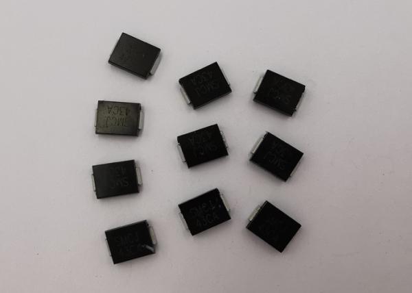
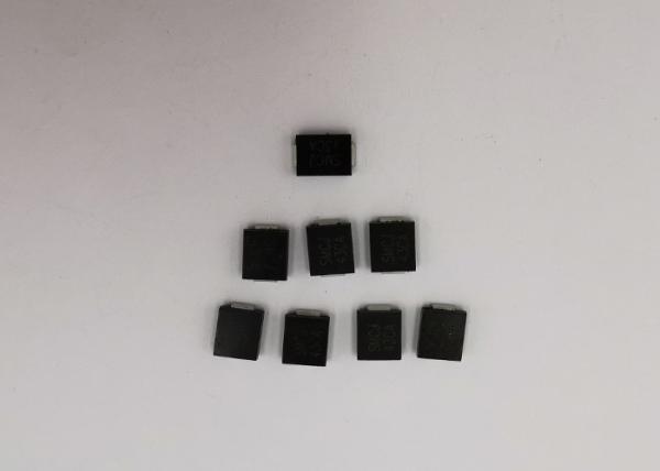
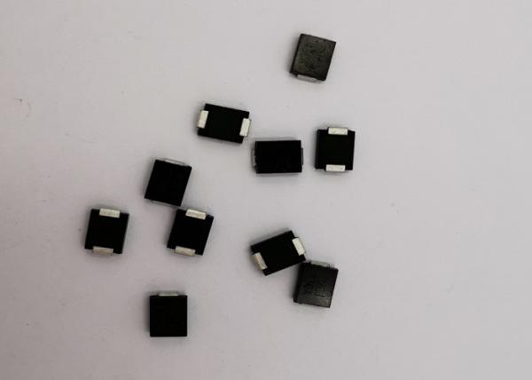
3.0 Amp 40V Surface Mount Schottky Rectifier Diode 30BQ040 DO-214AB
FEATURES
• Very low forward voltage drop
• Guard ring for enhanced ruggedness and long term reliability
• Halogen-free according to IEC 61249-2-21 definition
• Small foot print, surface mountable
• High frequency operation
• Meets MSL level 1, per J-STD-020, LF maximum peak of 260 °C
• Compliant to RoHS directive 2015/863/EC
DESCRIPTION
The 30BQ040 surface mount Schottky rectifier has been designed for applications requiring low
forward drop and small foot prints on PC boards. Typical applications are in disk drives, switching
power supplies, converters, freewheeling diodes, battery charging, and reverse battery protection.
MAJOR RATINGS AND CHARACTERISTICS | |||
SYMBOL | CHARACTERISTICS | VALUES | UNITS |
IF(AV) | Rectangular waveform | 3.0 | A |
VRRM | 40 | V | |
IFSM | tp = 5 μs sine | 2000 | A |
VF | 3.0 Apk, TJ = 125 °C | 0.43 | V |
TJ | Range | - 55 to 150 | °C |
VOLTAGE RATINGS | |||
PARAMETER | SYMBOL | 30BQ040-M3 | UNITS |
Maximum DC reverse voltage | VR | 40 | V |
Maximum working peak reverse voltage | VRWM |
ABSOLUTE MAXIMUM RATINGS | |||||
PARAMETER | SYMBOL | Test Condition | VALUES | UNITS | |
Maximum average forward current | IF(AV) | 50 % duty cycle at TL = 115 °C, rectangular waveform | 3.0 | A | |
50 % duty cycle at TL = 104 °C, rectangular waveform | 4.0 | ||||
Maximum peak one cycle non-repetitive surge current | IFSM | 5 μs sine or 3 μs rect. pulse | Following any rated load condition and with rated VRRM applied | 1600 | |
10 ms sine or 6 ms rect. pulse | 90 | ||||
Non-repetitive avalanche energy | EAS | TJ = 25 °C, IAS = 1.0 A, L = 12 mH | 6. | mJ | |
Repetitive avalanche current | IAR | Current decaying linearly to zero in 1 μs Frequency limited by TJ maximum VA = 1.5 x VR typical | 1.0 | A |
ELECTRICAL SPECIFICATIONS | |||||
PARAMETER | SYMBOL | Test Condition | VALUES | UNITS | |
Maximum forward voltage drop | VFM(1) | 3A | TJ = 25 °C | 0.57 | V |
6A | 0.76 | ||||
3A | TJ = 125 °C | 0.46 | |||
6A | 0.64 | ||||
Maximum reverse leakage current | IRM | TJ = 25 °C | VR = Rated VR | 0.5 | |
TJ = 125 °C | 30 | mA | |||
Maximum junction capacitance | CT | VR = 5 VDC (test signal range 100 kHz to 1 MHz), 25 °C | 230 | pF | |
Typical series inductance | LS | Measured lead to lead 5 mm from package body | 3.0 | nH | |
Maximum voltage rate of change | dV/dt | Rated VR | 10 000 | V/μs |
Note
(1) Pulse width = 300 μs, duty cycle = 2 %
THERMAL - MECHANICAL SPECIFICATIONS | ||||
PARAMETER | SYMBOL | Test Condition | VALUES | UNITS |
Maximum junction and storage temperature range | TJ (1), TStg | - 55 to 150 | °C | |
Maximum thermal resistance, junction to lead | RthJL (2) | DC operation | 12 | °C/W |
Maximum thermal resistance, junction to ambient | RthJA | 46 |
Drawing:
What can you from XUYANG?
Best service: with 10 years experience in exporting sales staff will service you.
High quality: help you to avoid purchasing risk.
Short delivery: help you to save time.
Competitive price: the price is not the lowest but the highest cost performance
OEM/ODM: we are confident we can meet you OEM/ODm requirements.