Aoi Pcb Assembly FR-1 PCBA Prototype Electronic Assembly Fabrication
Shenzhen Yideyi Technology Co., Ltd provide industry design, mechanical design, electronic design, hardware design, firmware development, software development, app development, PCB fabrication, PCB assembly, box-building, and one-stop turnkey solutions.
Turnkey Solutions
1. Electronic Design & Development
2. PCBA Prototyping
3. Quick-turn
4. Solid PCB Manufacturing and Assembly
5. Mix-Production
6. Cutting-edge Manufacturing
7. Exceptional Turn Time
8. Competitive Cost
9. Complete Confidentiality
10. Consulting of DFM/Design for Manufacturability
11. DFT/Design for Testability
12. Confirmation of EMI Control
13. Free to get some solutions for your electronic project as you need.
PCBA Capability
| | Normal FR4,Normal Tg FR4(Halogen free),High Tg FR4(Halogen free),HDI PCB material |
| | Rigid pcb(Backplane,HDI,High multi-layer blind&buried PCB,Embedded Capacitance) |
| | Blind&buried via type,HDI PCB |
| | Lead free,Leaded,aspect ratio,Max finished size,MIN finished size, PCB thickness, MAX high to gold finger |
Plating/coating thickness | Tin thickness,OSP, ENIG, Immersion Silver,Immersion Tin,Hard gold, Soft gold |
| | MAX thickness of mechanical hole 4mil/6mil/8mil,Min/Max laser drilling size,Finshed mechanical hole size |
| | Min Pad size for laser drillings,Min Pad size for mechanical drillings,Min BGA pad size,Pad size tolerance(BGA) |
| | MAX drilling tool size for via filled with Soldermask (single side) |
| | Min gap between mechanical hole wall and conductor (Local mixed pressure area) |
| | Layer counts,PCB size (Finished),MAX PCB size(Ceramic-substrate PCB),PCB thickness(Finished) |
| | Min space of the V-CUT does not reveal the copper ( Central Line of v-cut to internal/external circuits,H means board thickness) |
Technology Unique
YDY integrated solutions are unique forefront technologies, which including Industry Design, Mechanical Design, Hardware Development, Firmware Development, Software Development, App & Api Development, and Electronic Manufacturing Service (EMS).
(DLP projector, Advertising Player, eBook Reader, Type C solutions, Embedded system products, Power project,Quick charging, Wireless charging, Solar Power solution, etc)
For complexity and rapid updating requirements, offer our comprehensive set of value-added quick realization services. YDY has some technical experts,with flexibility, competency and scalable capacity to handle all of project needs.

PCB Manufacturing
Offer: Rigid PCB; Flexible PCB; Rigid-flex PCB; HDI PCB; Gold-Plated PCB; High Frequency PCBs; Aluminum PCB; Copper Base Circuit Board; High TG PCB; Heavy Copper PCB...
FAQ:
Q1. How to you make the impedance calculation?
The impedance control system is done using some test coupons, the SI6000 soft and the CITS 500s equipment from POLAR INSTRUMENTS.
The equipment measures the impedance on a representative track configuration coupon of which the client has given us a determinate value and tolerance.
Q2. What kind of PCB file format can you accept for production?
Gerber, PROTEL 99SE, PROTEL DXP, CAM350, ODB+(.TGZ)
Q3. How do we ensure quality?
Our high quality standard is achieved with the following.
1. The process is strictly controlled under ISO 9001:2008 standards.
2. Extensive use of software in managing the production process
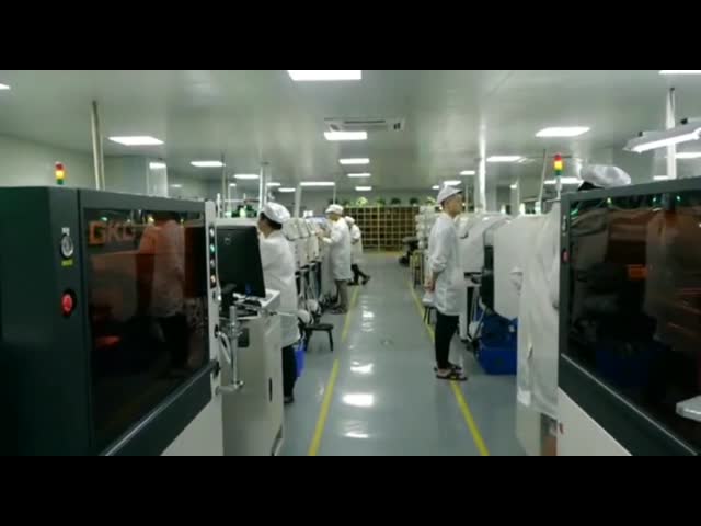
3. State-of-art testing equipments and tools. E.g. Flying Probe, X-ray Inspection, AOI (Automated Optical Inspector) and ICT (in-circuit testing).
4. Dedicated quality assurance team with failure case analysis process
5. Continuous staff training and education
Q4. How can we guarantee you receive an good quality product?
For PCB, we will use Flying Probe Test, E-test etc. for it.
For PCBA, we need you to offer us a method or test fixture for the function test.Before that, our inspectors will use microscope and X-ray to check the IC footwelding or bad solder etc.
Q5. What’s the key equipments for HDI manufacturing?
Key equipment list is as following: Laser drilling machine, Pressing machine, VCP line, Automatic Exposing machine, LDI and etc.
Q6. What’s the typical process flow for multi-layer PCB?
Material cutting → Inner dry film → inner etching → Inner AOI → Multi-bond→ Layer stack up Pressing → Drilling → PTH → Panel Plating → Outer Dry Film → Pattern Plating → Outer etching → Outer AOI → Solder Mask → Component Mark → Surface finish → Routing → E/T → Visual Inspection.